
In the realm of electronics, Printed Circuit Boards (PCBs) are the unsung heroes, quietly powering our devices and gadgets. These intricate boards serve as the backbone of virtually every electronic device we encounter in our daily lives. In this blog, we’ll embark on a journey through the world of PCBs, uncovering their significance, the manufacturing process, and their role in shaping our technological landscape.
The Heartbeat of Electronics
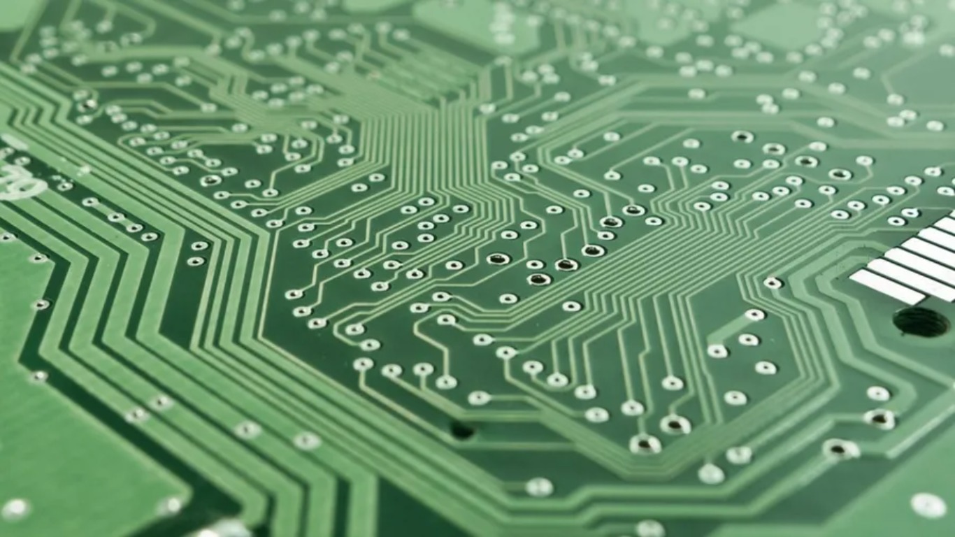
What are Printed Circuit Boards?
At their core, PCBs are flat, rigid boards made of non-conductive material, often fiberglass, with thin layers of conductive material etched onto them. These conductive pathways act as the “circulatory system” of electronic devices, facilitating the flow of electricity and enabling components to communicate with one another.
Manufacturing Marvels: How PCBs Come to Life
Design and Schematic
The journey of a PCB begins with a meticulous design phase. Engineers create a schematic, outlining the arrangement of components and their interconnections. This serves as the blueprint for the physical PCB.
Layering and Substrate
PCBs are typically composed of multiple layers, each with its own conductive pathways. These layers are sandwiched together with insulating material, forming a composite substrate. The arrangement of these layers depends on the complexity and functionality of the final device.
Etching and Tracing
Once the layers are stacked, the conductive pathways are etched onto the board. This process removes unwanted copper, leaving behind precise traces that connect the various components.
Component Mounting
After the traces are in place, electronic components such as resistors, capacitors, and integrated circuits are soldered onto the board. These components are carefully positioned based on the schematic, with automated machines often used for precision.
Quality Control and Testing
Rigorous quality control measures are in place to ensure the PCB functions as intended. Automated testing equipment checks for electrical continuity, shorts, and other potential issues.
Shapes, Sizes, and Types
Varieties of PCBs
PCBs come in various forms, tailored to specific applications. Single-layer PCBs are used in simpler devices, while multi-layer PCBs accommodate more complex electronics. Flexible PCBs, as the name suggests, can bend to fit unconventional shapes.
Beyond the Basics: Advanced PCB Technologies
Surface Mount Technology (SMT)
SMT revolutionized PCB assembly, allowing for smaller components and denser circuitry. This technology enables more compact and lightweight electronic devices.
Through-Hole Technology (THT)
While somewhat older, THT remains relevant for components that require sturdier connections. It involves inserting component leads through holes in the PCB and soldering them on the other side.
Conclusion: Empowering the Electronic Ecosystem
Printed Circuit Boards are the silent heroes of our electronic age, facilitating the seamless operation of devices that have become integral to our daily lives. From smartphones to spacecraft, PCBs form the foundation upon which modern technology stands. Understanding their significance allows us to appreciate the intricate engineering and craftsmanship that go into every electronic marvel we encounter. As we continue to push the boundaries of innovation, PCBs will undoubtedly play an even more pivotal role in shaping our technological future.
Thank you for reading this post, don't forget to subscribe our Youtube Channel.